Products & Services

Phase 1 Planned Products

At launch, Hudson Hi-Tech will prioritize the high-volume, high-impact substrates required for today’s core semiconductor, power, and communications markets. These Phase 1 products are being developed for scalable manufacturing in our planned New York facility.

Cleanroom-Ready Monocrystalline Silicon Wafers

High-purity, precision-engineered monocrystalline silicon wafers will be manufactured to meet stringent cleanroom and semiconductor fabrication standards. These wafers will offer exceptional uniformity, low defect density, and excellent thermal stability—ideal for ICs, sensors, MEMS, and advanced electronic devices.

Sizes in Focus:

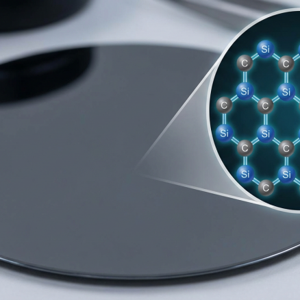
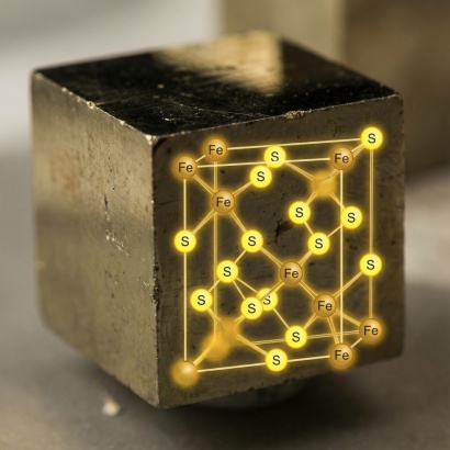
Silicon Carbide (SiC) Wafers

High-Voltage, High-Efficiency Material for Power Devices

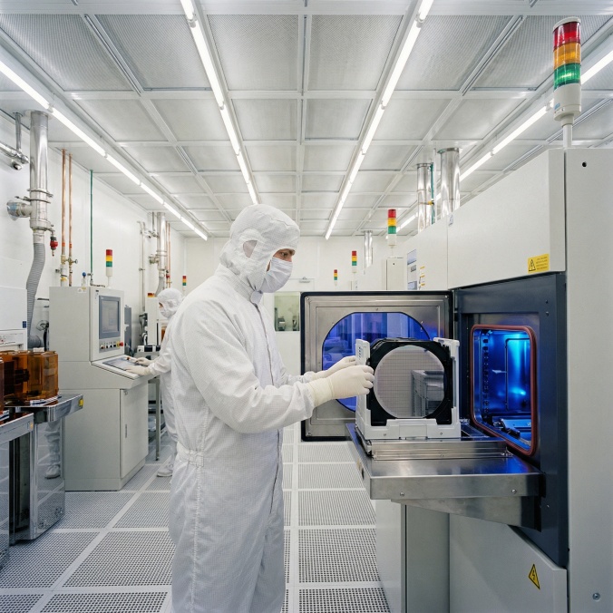
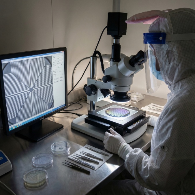
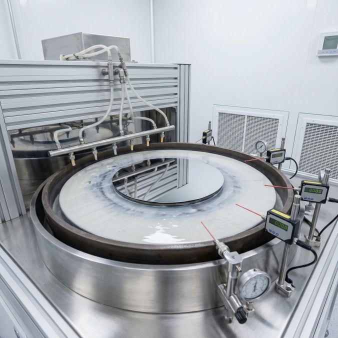
Hudson Hi-Tech is planning SiC wafer production to support high-temperature, high-voltage, and high-efficiency power device applications. These wafers are being developed for exceptional thermal conductivity and switching performance, crucial for electric mobility, energy infrastructure, and industrial power electronics. As global demand for power semiconductors grows, SiC remains one of the most future-ready materials in our roadmap.

Future R&D Roadmap

Beyond Phase 1 production, Hudson Hi-Tech is building a structured R&D pipeline around compound semiconductors and emerging materials. These platforms are the focus of ongoing development, prototyping, and collaboration with research and industry partners, with the goal of enabling next-generation devices over time.

Germanium Wafers

High-Purity Substrates for Infrared, Optoelectronic & Power Applications

Germanium wafers are being developed as high-purity substrates with exceptional carrier mobility and infrared transparency, making them well suited for high-performance photodetectors, solar cells, and advanced optoelectronic devices. Their uniform crystalline structure supports superior signal sensitivity and efficient energy capture, positioning germanium as a strategic material for next-generation sensing and communication technologies.

High-Power Gallium Nitride (GaN) Wafers

Wide-Bandgap Platform for Fast, Compact Power Systems

Hudson Hi-Tech’s GaN wafer roadmap focuses on substrates that enable ultra-fast, high-efficiency power conversion in compact form factors. These materials are being targeted for RF systems, power electronics, fast chargers, and communication hardware. As demand for energy-efficient electronics continues to rise, GaN is expected to complement silicon and SiC by delivering superior performance-per-watt in advanced designs.

Indium Phosphide (InP) Wafers

Premium III–V Substrates for High-Speed Photonics & Telecom Devices

Indium phosphide wafers form part of Hudson Hi-Tech’s future portfolio for ultra-high-frequency electronic and photonic applications, including 5G/6G systems, high-speed lasers, and advanced communication hardware. With excellent electron mobility and direct bandgap properties, InP enables low-loss transmission, efficient light emission, and exceptional performance in leading-edge optoelectronic components.

Antimonide-Based & Bismuthide-Based Semiconductors

Specialized III–V Materials for Infrared & High-Mobility Applications

These advanced compounds are currently positioned within Hudson Hi-Tech’s R&D roadmap for infrared sensors, photonics, and high-mobility semiconductor devices. Their unique bandgap properties unlock performance in extreme or niche environments. Adoption of these materials is expanding in aerospace, defense, and precision optical systems, and Hudson Hi-Tech aims to support this growth through targeted development and collaboration.

Gallium Arsenide (GaAs) Wafers

High-Mobility Substrates for RF, Aerospace & High-Efficiency Solar

GaAs wafers are being explored as high-mobility substrates offering excellent electron transport and high-temperature stability. They are suited for RF amplifiers, satellite communication systems, and multi-junction solar cells. Their direct bandgap and low noise characteristics support the high-power, high-frequency performance required in advanced aerospace, defense, and energy-efficient electronic technologies.

Graphene Wafers

Ultra-High Mobility Platform for Next-Generation Nanoelectronics

Graphene materials in Hudson Hi-Tech’s roadmap are focused on exceptional electrical mobility, mechanical strength, and thermal performance. These platforms are intended for nanoelectronics, sensors, advanced composites, and transparent conductive devices. As global research accelerates, graphene is expected to remain a key enabler for next-generation high-speed and flexible electronics.

Pyrite (FeS₂) Semiconductor Material

Sustainable Semiconductor Material for Emerging Green Technologies

Pyrite wafers are being evaluated as a cost-effective, earth-abundant platform for sustainable semiconductor applications. Their optical absorption and material availability make them promising candidates for photovoltaics and experimental electronics. With rising interest in green technologies, pyrite is under consideration as a pathway toward scalable clean-energy devices.

Planned Technical & Manufacturing Services

Hudson Hi-Tech is designing technical and manufacturing services to support end-to-end wafer processing with precision, consistency, and scalability. As the facility becomes operational, these processes will strengthen material quality and prepare wafers for high-performance semiconductor applications.

Surface Preparation & Coating

Acid Coating & Dipping for Defect-Ready Wafer Surfaces

Hudson Hi-Tech plans to implement surface-treatment processes—combining precision acid coating and controlled dipping—to prepare wafers for high-yield fabrication. These treatments are designed to ensure uniform cleaning, controlled etching, and enhanced surface adhesion for subsequent process layers. This step will be essential for reducing defects, improving consistency, and achieving stable downstream device performance.

Material Layer Formation

Deposition Techniques for Consistent Thin-Film Layering

Advanced deposition methods will be used to form ultra-uniform thin films essential for device architecture. These controlled layers will enable the electrical, optical, and structural performance required in semiconductor manufacturing. With high repeatability and precision, Hudson Hi-Tech’s planned deposition services are intended to support scalable production across multiple device types.

Material Engineering & Modification

Compounding & Doping for Customized Material Properties

Through specialized compounding and atomic-level doping, Hudson Hi-Tech aims to tailor material compositions to meet precise electrical and performance specifications. These processes will modify conductivity, carrier concentration, and other critical parameters required for advanced semiconductor applications, enabling engineered material behavior optimized for both high-performance and emerging device technologies.

Precision Lapping

High-Accuracy Surface Planarization for Wafer Uniformity

Planned precision lapping services will deliver exceptionally flat, smooth wafer surfaces essential for tight-tolerance manufacturing. By removing micro-level variations, lapping will enhance structural stability and prepare wafers for further polishing or deposition steps. This will help ensure consistent device fabrication with improved efficiency and long-term reliability.

Powering the Technologies That Shape Tomorrow

From AI to aerospace, Hudson Hi-Tech’s planned precision wafer substrates are being designed to support breakthrough innovations across critical industries. Target applications include autonomous vehicles, data-center AI accelerators, and defense-grade communication systems—all of which rely on high-performance semiconductor foundations. As the facility comes online, Hudson Hi-Tech aims to serve the technology ecosystems that power modern infrastructure and intelligent systems.

Defense & Aerospace

Mission-critical semiconductor components for radar systems, satellite communications, guidance platforms, and defense electronics.

5G & Telecommunications

High-frequency substrates enabling 5G infrastructure, base stations, network equipment, and communications backbone connectivity.

Healthcare & Medical Devices

Precision substrates for diagnostic equipment, medical imaging systems, patient monitoring, and future implantable electronics.

Clean Energy & Solar

Photovoltaic-grade and advanced materials supporting solar cell manufacturing, renewable energy conversion, and sustainable power solutions.

Internet of Things (IoT)

Sensor arrays, smart home devices, industrial IoT systems, and connected infrastructure transforming modern environments.

Cloud Computing

High-performance substrates for server processors, accelerators, memory chips, storage systems, and data center infrastructure.

Hudson Hi-Tech manufactures premium silicon wafers for the semiconductor industry.  American made. CHIPS Act backed. Future ready.

Contact Us

No 60 Skillman Avenue.
Apartment no 505, Jersey City 07306

© Copyright 2025 Hudson Hi-Tech | Created By Reverspitch