
Redefining American Semiconductor Manufacturing
Hudson Hi-Tech is establishing America’s newest semiconductor foundry in New York. Upon operational launch, we will deliver comprehensive semiconductor manufacturing solutions with precision and reliability. Our facility will power AI, autonomous vehicles, defense systems, and 5G infrastructure by leveraging over 20 years of specialized metallurgy expertise from our founding team. Founded by industry veterans, we view manufacturing not just as science, but as art—a regional partner you can trust for advanced semiconductor solutions.
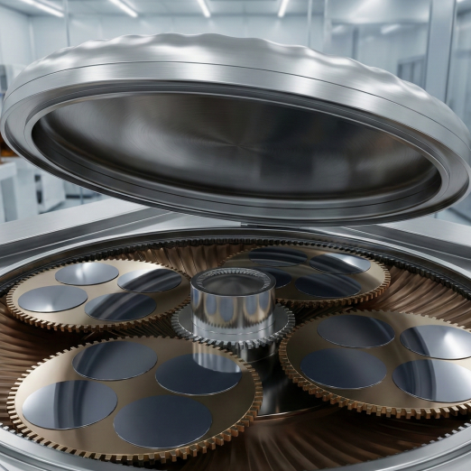
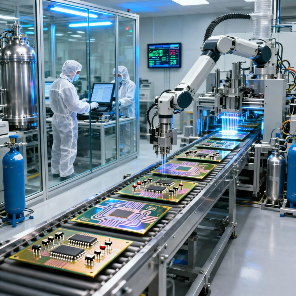
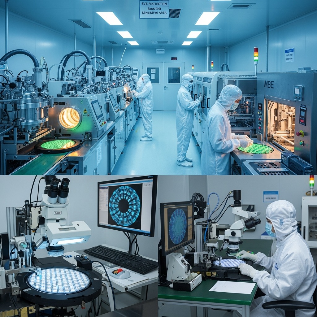
At the heart of our planned facility is the classic Czochralski (CZ) method—a proven technique for producing semiconductor-grade silicon ingots with exceptional purity levels. We will implement meticulous quality protocols at every production stage to meet your precision requirements. Through inland manufacturing and local sourcing, our facility will provide supply chain resilience and reduced lead times for domestic industries. Silicon features four valence electrons and crystallizes in a diamond cubic structure, creating the strong mechanical properties and atomic lattice precision essential for advanced semiconductor applications. Our multi-diamond wire cutting technology will ensure consistent wafer thickness and optimal surface quality, while our lapping processes will deliver exact specifications for photolithography and circuit deposition, achieving total accuracy from atomic structure to final product for local production and usage.
Hudson Hi-Tech will manufacture hyper-pure semiconductor-grade silicon ingots with 99.9999% purity, transforming them into flawless wafers through advanced diamond wire cutting, custom grinding, and mirror-finish polishing processes.
Classic Czochralski method producing semiconductor-grade materials with 99.9999% purity.
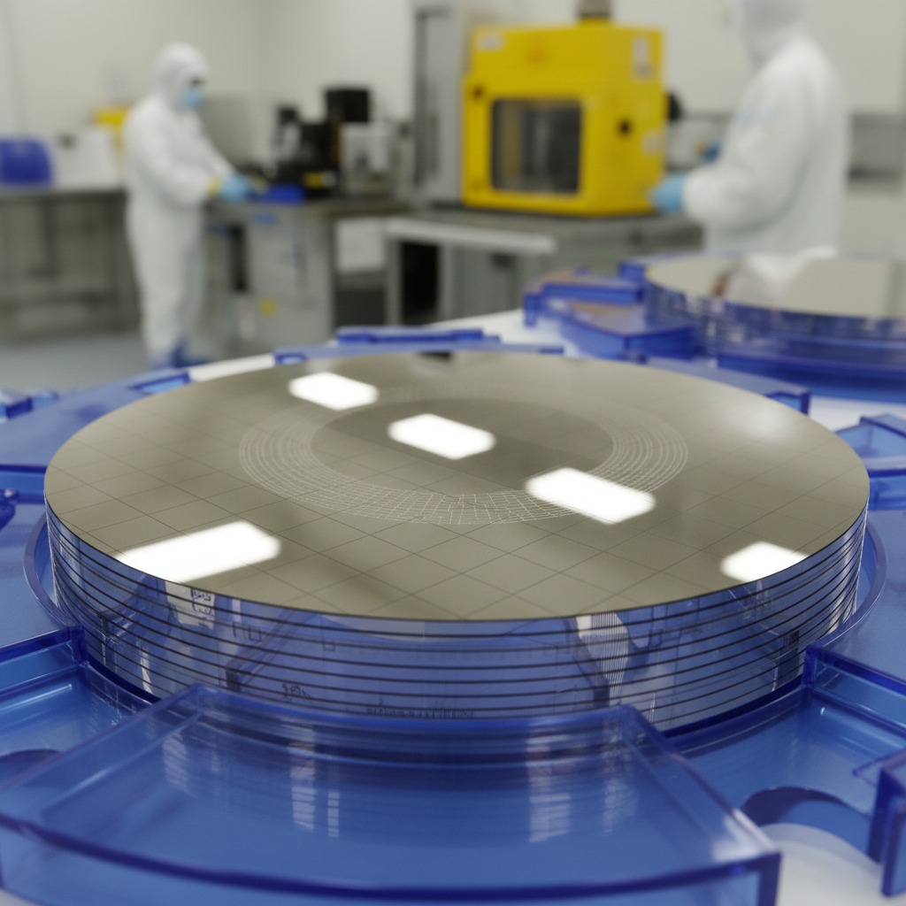
High-quality semiconductor wafers with consistent thickness and exceptional uniformity for advanced applications.
Tailored specifications meeting exacting standards for photolithography and circuit deposition.
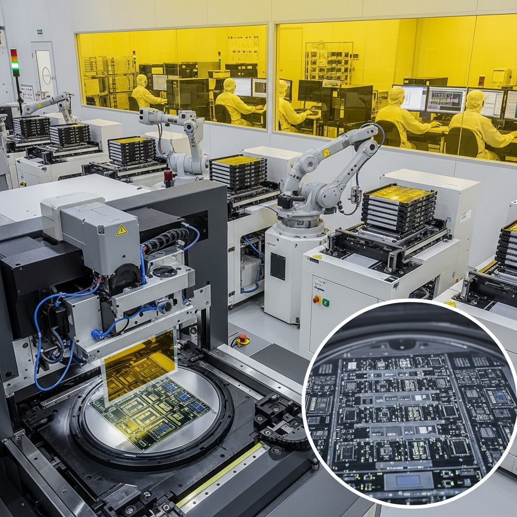
Our competitive edge will extend beyond location. With state-of-the-art pullers, precision diamond wire cutting, and custom grinding processes, our facility will deliver wafers that meet frontier technology standards while maintaining cost efficiency through economies of scale. We will maintain a tightly integrated quality loop that links material sourcing, growth, slicing, and finishing into one continuous flow. This integrated approach will allow us to scale output without ever compromising on consistency.
Will reduce foreign dependency and supply chain risk
Planned expansion to 5M wafers monthly
NY's chip corridor will enable faster growth
Frontier tech company supporting industry growth
20+ years of specialized crystal pulling experience
Applying for CHIPS Act Funding
Our wafers will accelerate innovation in electronics, optoelectronics, and power-device manufacturing. These next-generation applications form the backbone of semiconductor growth and represent pivotal opportunities for expanding high-value market segments.
Building the Core Elements of Electrical Control
Manufacturers in this segment produce fundamental components—transistors, diodes, rectifiers, and high-voltage power devices—that drive everything from consumer electronics to industrial systems. Our wafers will deliver the precision and stability required for consistent electrical performance. This will enable manufacturers to achieve higher efficiency, lower losses, and improved reliability across power applications.
High-Frequency and High-Power Device Innovators
This segment develops advanced MOSFETs, FETs, and HEMTs used in RF communication, high-speed switching, and next-generation power systems. Our wafers will provide the uniformity and material integrity essential for high-frequency stability. These qualities will help device makers push boundaries in performance, thermal handling, and power density.
Designers of Intelligent and High-Density Chip Systems
From processors and memory units to mixed-signal and logic ICs, these manufacturers create the computing backbone of modern technology. Our wafers will support fine patterning, high circuit density, and consistent electrical characteristics. This will ensure dependable performance for complex chip architectures across diverse applications.
Enabling Light-Driven and Optical Technologies
LEDs, laser diodes, and photonic sensors rely on high-purity wafer substrates to deliver optical accuracy and efficiency. Our wafers will ensure stable light emission, precise signal detection, and long-term reliability. These qualities will help manufacturers build advanced lighting, communication, and imaging solutions.
Hudson Hi-Tech manufactures premium silicon wafers for the semiconductor industry. American made. CHIPS Act backed. Future ready.
No 60 Skillman Avenue.
Apartment no 505, Jersey City 07306