Investors

Wafers Target
0 M+
Full Phase Revenue Potential
$ 0 B
Years Expertise
0 +
First Phase Funding Target
$ 0 M

The Problem

The global semiconductor market is projected to exceed 1 trillion dollars by 2030, yet only 31 foundries serve 5.5 billion end-users worldwide. The U.S. currently produces around 10% of global semiconductors despite massive domestic demand, creating critical supply chain vulnerabilities that have cost industries billions in losses. The 2021 chip shortage alone is estimated to have resulted in approximately 210 billion dollars in automotive losses and 12–15% production drops across consumer electronics.

Enabling U.S. Innovation with Reliable, Scalable Manufacturing

Enabling U.S. Innovation with Reliable, Scalable Manufacturing

Our Solution

Hudson Hi-Tech is planning a fully domestic semiconductor manufacturing hub in New York to help address this global foundry bottleneck. The proposed 180,000 sq. ft. advanced facility is being designed to ultimately support production of up to 1.5 million hyper-pure silicon wafers per month using proven Czochralski technology, supplying high-performance computing, power electronics, and national defense programs.

New York’s semiconductor corridor offers strong structural advantages—abundant clean energy, extensive water resources, efficient logistics, and one of America’s most robust semiconductor-ready workforce pipelines—reinforced by major regional investments such as Micron’s announced megafab in Clay and the Albany NanoTech NSTC.

The planned operations will deploy up to 50 high-precision crystal pullers producing 99.9999%-pure silicon ingots, followed by diamond‑wire slicing and custom grinding and polishing for end‑to‑end quality control. This integrated approach is being engineered so that wafers can meet the stringent requirements of AI processors, automotive sensors, 5G infrastructure, and defense electronics.

At an illustrative average selling price of 125 dollars per wafer, the full Phase capacity described above would represent approximately 187.5 million dollars in monthly turnover—about 2.25 billion dollars annually. These figures are forward‑looking projections intended to outline the long‑term economic potential of the facility rather than current operating results.

Current Stage, Timeline & Funding Overview

Hudson Hi-Tech is currently in the pre-construction planning stage, with work underway on detailed design, site evaluation, and stakeholder engagement. To execute this roadmap, Hudson Hi-Tech is targeting a phased capital structure that combines private investment, strategic partnerships, and potential federal and state incentives.

2026Site Selection & Design
2027Permitting & Groundbreaking
2028Tool Install & Pilot
2029Phase 1 Production Ramp

Comprehensive Investment Documentation

Hudson Hi-Tech provides accredited investors with a comprehensive set of due diligence materials that detail the project’s technical, financial, and regulatory foundations which will be available upon request and after signing NDA.

Project Location Analysis

Geotechnical, infrastructure, and economic justification for proposed plant placement.

SWOT Analysis

Strategic assessment of strengths, weaknesses, opportunities, and key risk factors.

Manufacturing Process Documentation

Raw material analysis, quality parameters, and preliminary supplier strategy.

Financial Models & Planned Economics

Forward‑looking financial models with sensitivity analysis, profitability ratios, and break‑even scenarios.

Market Study

Demand forecasts, supply landscape, and competitive positioning across core end markets.

Regulatory Compliance

CHIPS Act eligibility planning, environmental and zoning pathways, and safety and regulatory compliance frameworks.

Strategic Positioning for Market Leadership

Hudson Hi-Tech’s strategy is built around six critical advantages that, if executed as planned, are expected to position the company competitively within the U.S. semiconductor manufacturing landscape. These pillars combine favorable policy alignment, proven process technology, regional positioning, and differentiated customer focus.

CHIPS Act Alignment

Hudson Hi-Tech is structuring its project to align with CHIPS Act eligibility criteria, including domestic manufacturing, workforce development, and R&D collaboration. The U.S. federal government has announced up to 280 billion dollars in authorized support across incentives, tax credits, and research initiatives for the broader industry, with the U.S. projected to capture roughly 28% of global semiconductor capital expenditures.

Hudson Hi-Tech intends to pursue applicable CHIPS Act and related programs as part of its overall capital strategy but does not represent that any specific grant or subsidy has been awarded at this time.

Proven Technology

The planned facility is centered on the classic Czochralski method, underpinned by more than 28 years of the CTO’s experience producing 99.9999%-purity silicon ingots. This mature, widely adopted process provides a stable foundation for scaling high‑quality wafer output while supporting continuous improvement and future integration of advanced materials.

First-Mover Advantage

Hudson Hi-Tech aims to become one of the first next‑generation semiconductor foundries of its kind in New York in decades, positioning the company to capture regional demand, talent, and ecosystem support. By locating within the state’s emerging semiconductor corridor, the project is designed to complement large anchor investments and help build a resilient, U.S.-based supply chain.

Target Customer Segments

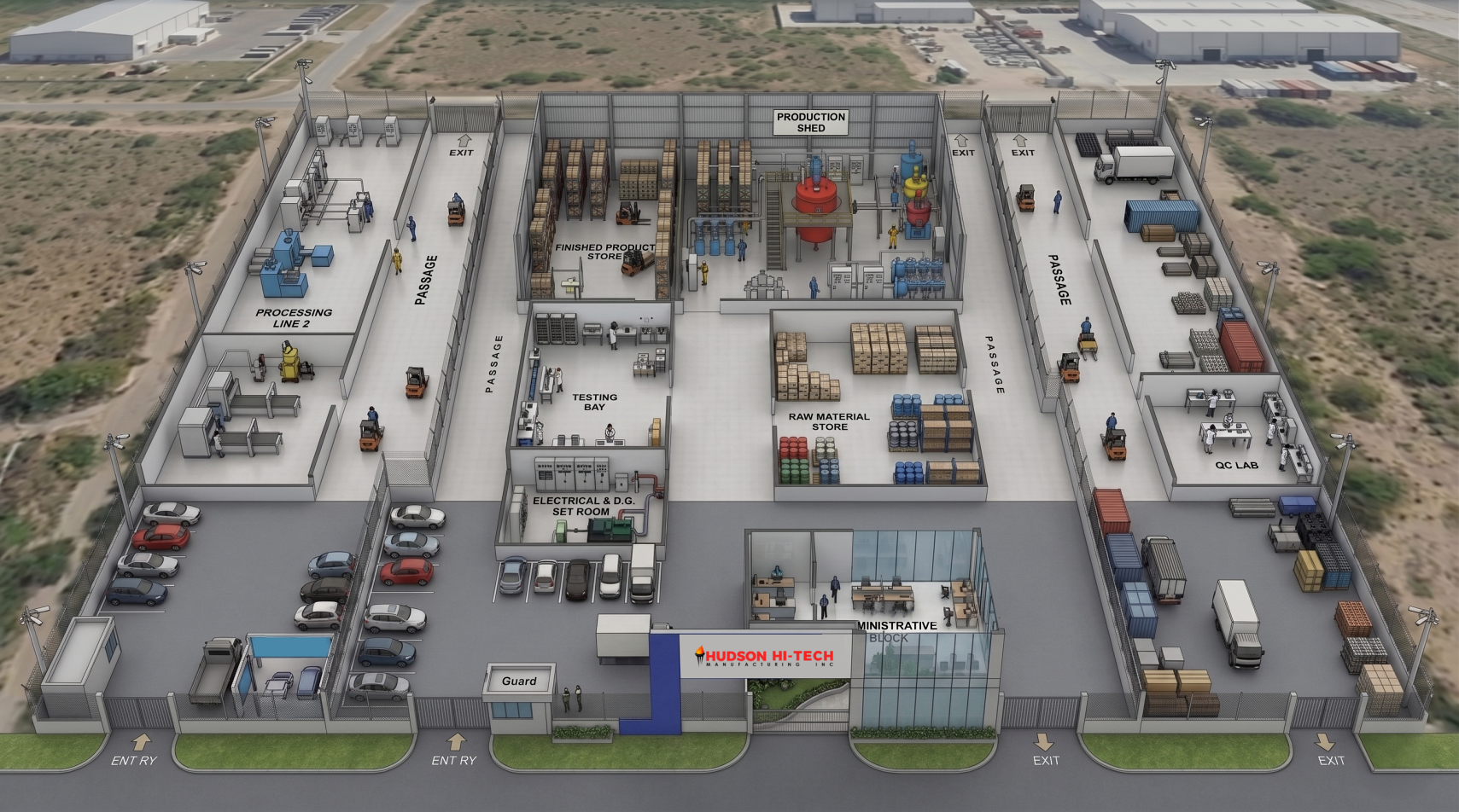
Hudson Hi-Tech is being positioned to serve high‑value technology segments that rely on advanced wafer substrates, rather than focusing on any single end customer. Target industries include:

  • Autonomous and electric vehicles

  • High‑performance and AI computing

  • Aerospace and space systems

  • Consumer and industrial electronics

  • Memory, storage, and data-center infrastructure

  • Defense and government technology programs

Leading companies in these sectors—such as major EV manufacturers, AI chip designers, aerospace organizations, and large semiconductor producers—represent the type of ecosystem partners Hudson Hi-Tech intends to engage as the facility advances from planning to production.

Hudson Hi-Tech manufactures premium silicon wafers for the semiconductor industry.  American made. CHIPS Act backed. Future ready.

Contact Us

No 60 Skillman Avenue.
Apartment no 505, Jersey City 07306

© Copyright 2025 Hudson Hi-Tech | Created By Reverspitch